Semiconductor Test Equipment (IC Tester)
Semiconductor Tester
Equipment to determine the pass/fail of devices in the wafer inspection process and the final inspection process after packaging.
MJC can provide both hard and soft test solutions to suit your needs, from IC semiconductor development and defect analysis to mass production.
We will develop custom testers and test systems with selected functions to suit the test environment or budget.
-
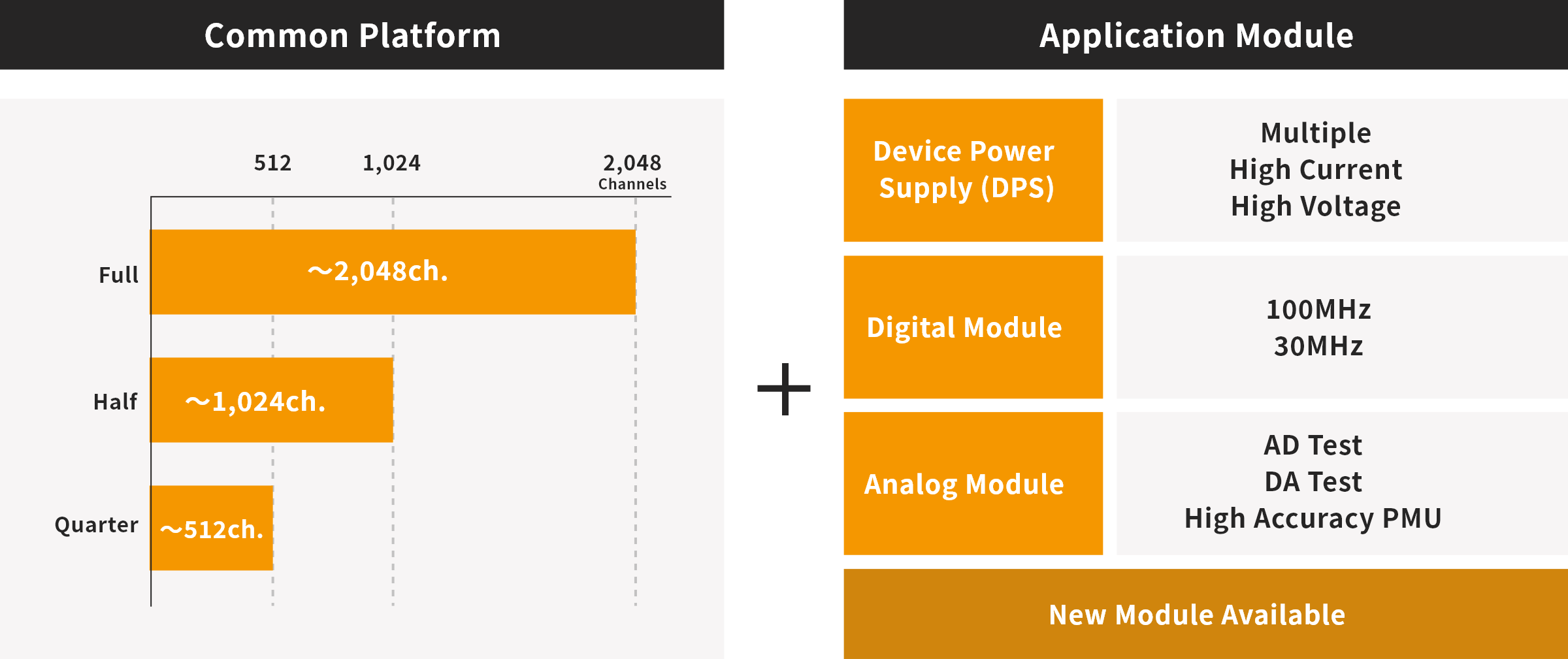
01New test modules can be provided on demand to test a wide range of devices
-
02Building test solutions for various type of devices or by adding software to meet needs
-
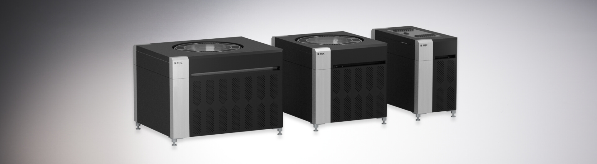
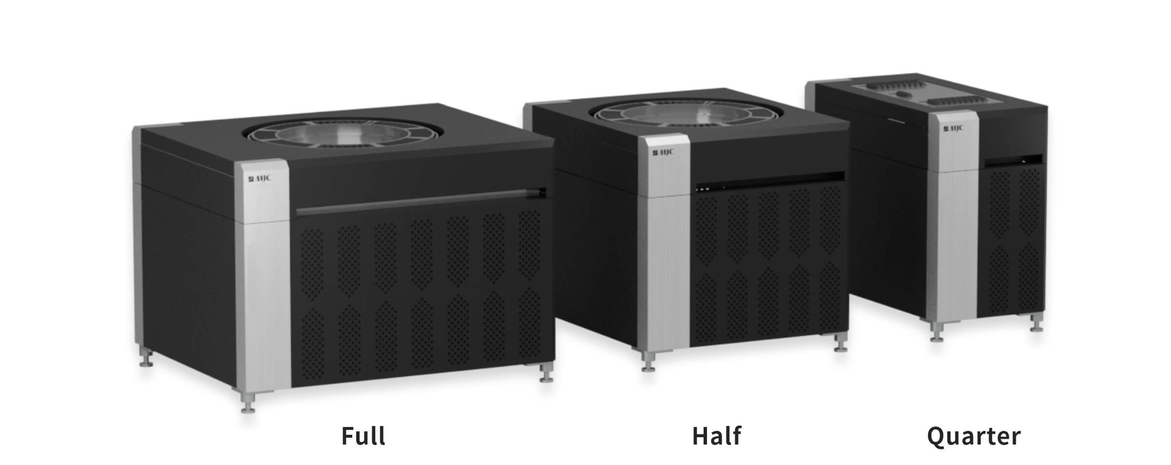
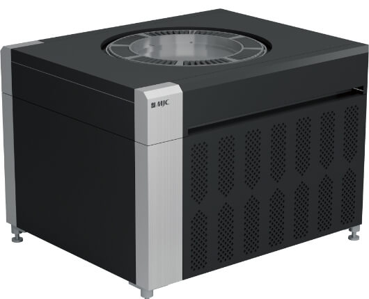
03The Main Body can be selected from 3 types (Full/Half/Quarter) depending on the test modules configuration
-
04Space-saving with built-in power supply and PC control in the housing Platform
depending on user device and test environment, we have a lineup of three types of common platformed main bodies.
What is Semiconductor Test Equipment (IC Tester)?
Semiconductor test equipment (IC tester), or automated test equipment (ATE), is a system for giving electrical signals to a semiconductor device to compare output signals against expected values for the purpose of testing if the device works as specified in its design specifications.
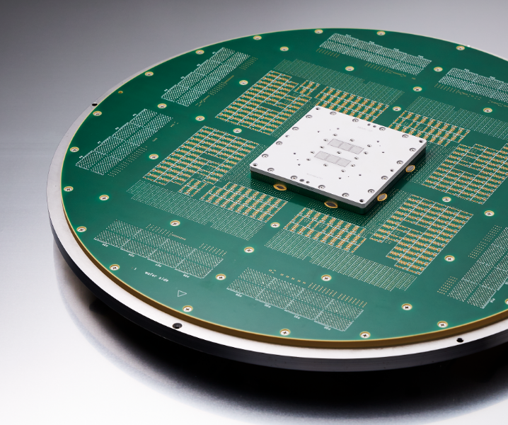
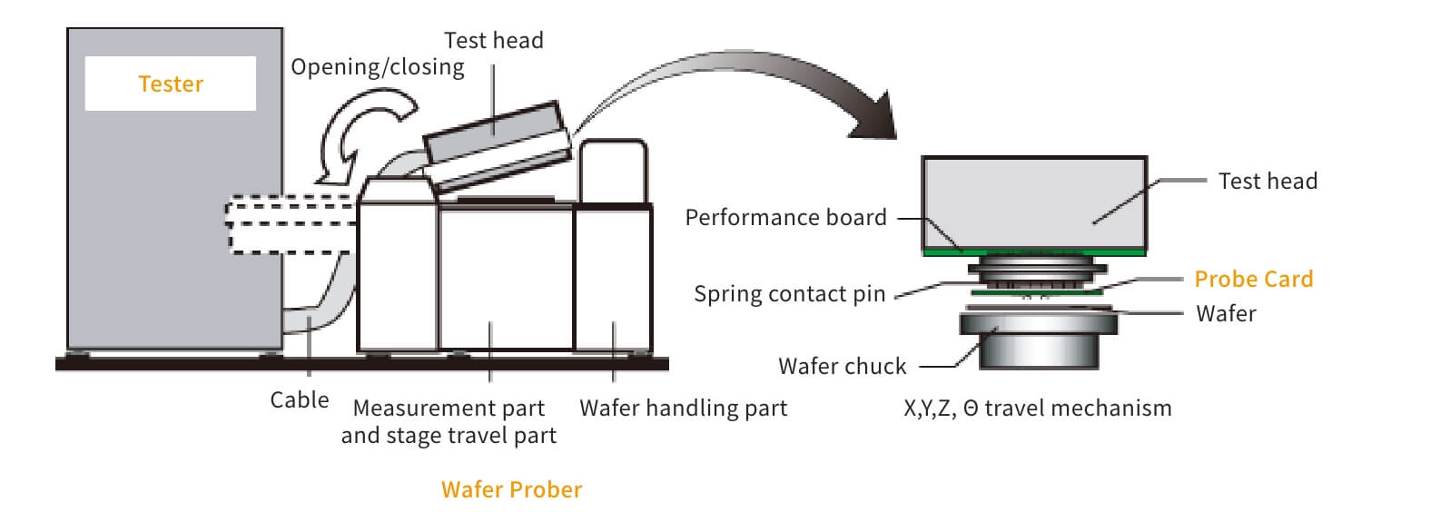
Testers are roughly categorized into logic testers, memory testers, and analog testers. Normally, IC testing is conducted at two levels: the wafer test (also called die sort or probe test) that tests wafers, and the package test (also called final test) after packaging. Wafer testing uses a prober and a probe card, while package testing uses a handler and a test socket, together with a tester.
【Logic testers】
【Wafer Test System】
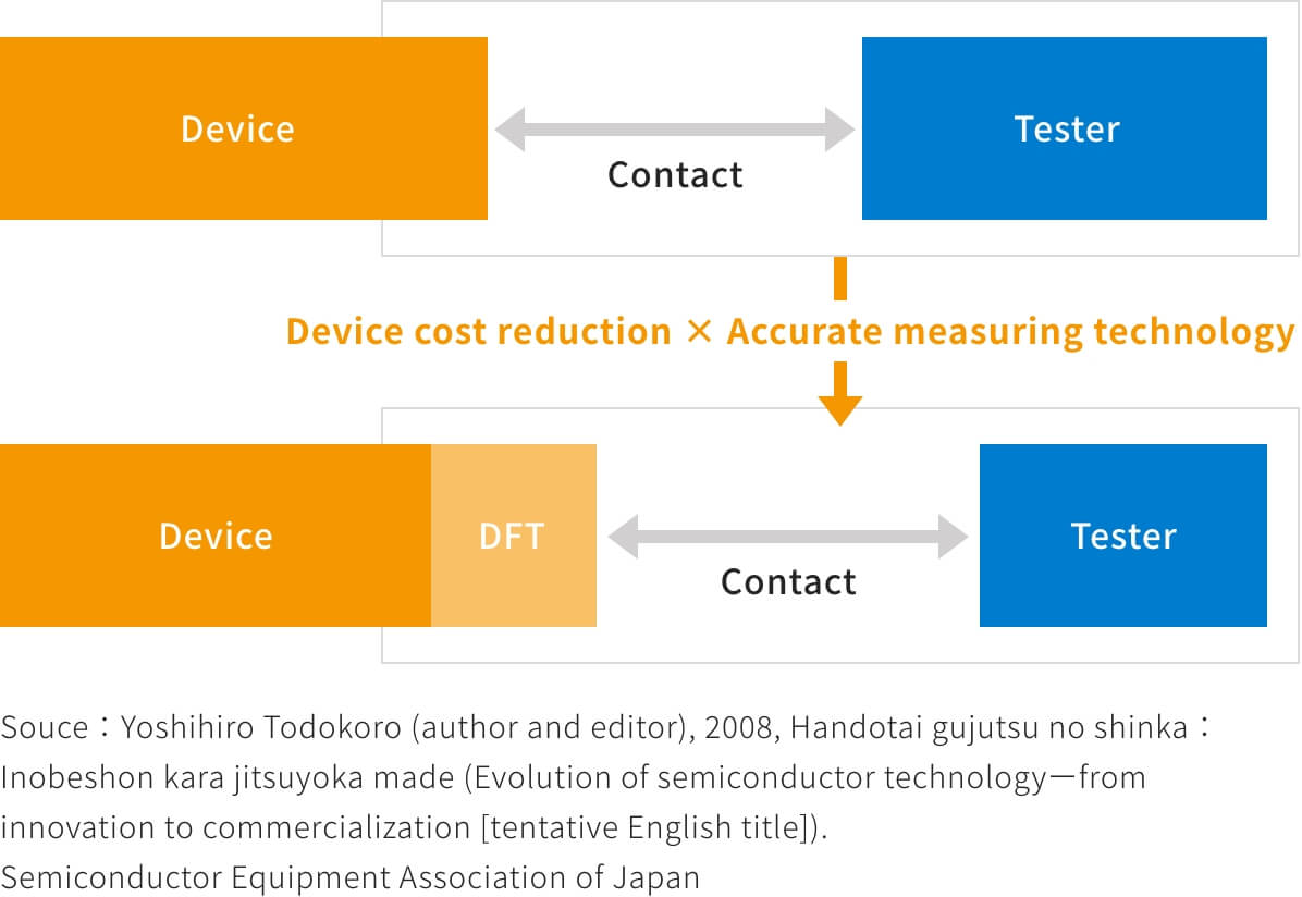
What is a DFT?
From the initial phase of IC design, we take ease of test into consideration when the circuit structure and is built-in.
We can accurately test in a short time and expect to reduce test cost.
What is a BIST?
BIST (Built-in Self Test) is one of the DFT technologies.
This is a method in which some of the functions originally provided by a tester are incorporated into the IC's circuitry, and the IC itself performs a self-test.
BIST circuitry includes functions such as generating test patterns to be applied to the circuit under test, compressing output patterns from the test object, and comparing the compressed patterns with expected values.
The functions required for the tester are limited, and many ICs can be tested at the same time, so test costs can be reduced.
BIST circuits include memory BIST for memory testing and logic BIST for logic circuit testing.
What is a SCAN test?
Scan testing is also DFT technique that is one of the methods for testing logic circuits.
It is one of the structural inspections used to detect faults in a mode in which the logic value is always 1 or 0 due to the opening or shorting of circuits inside the IC. During the scan test, a chain of FF (flip-flops) called a scan chain for testing is configured inside the IC. The test pattern data from the tester is sent to the circuit block under test via the FF chain, and the response reflecting the internal state of the test target is retrieved via the FF chain.
By comparing it with the pre-assumed response pattern, internal fault points can be detected.
By assuming a failure model in advance and automatically generating a pattern that makes it easier to identify defects from circuit design data, it is possible to perform tests with a high failure detection rate in a short time even for large-scale ICs.