Our Business
- Semiconductor Division
- FPD Division
Semiconductor Division
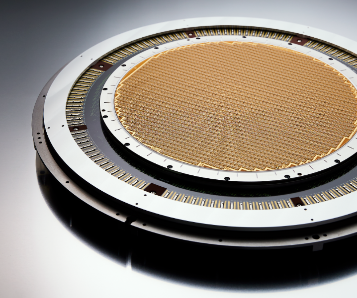
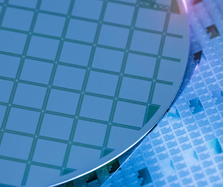
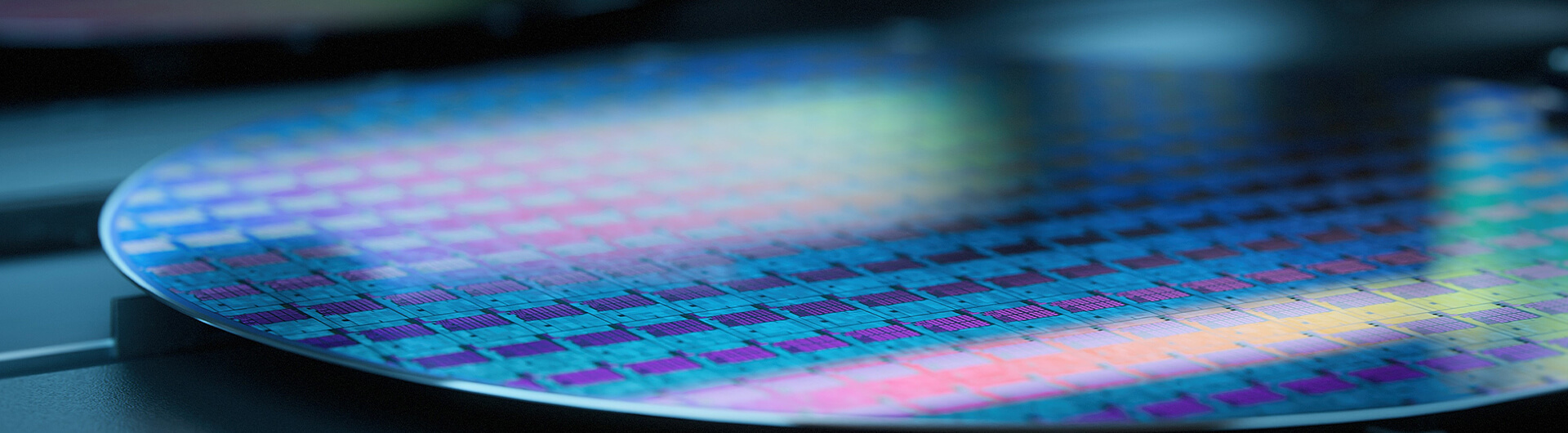
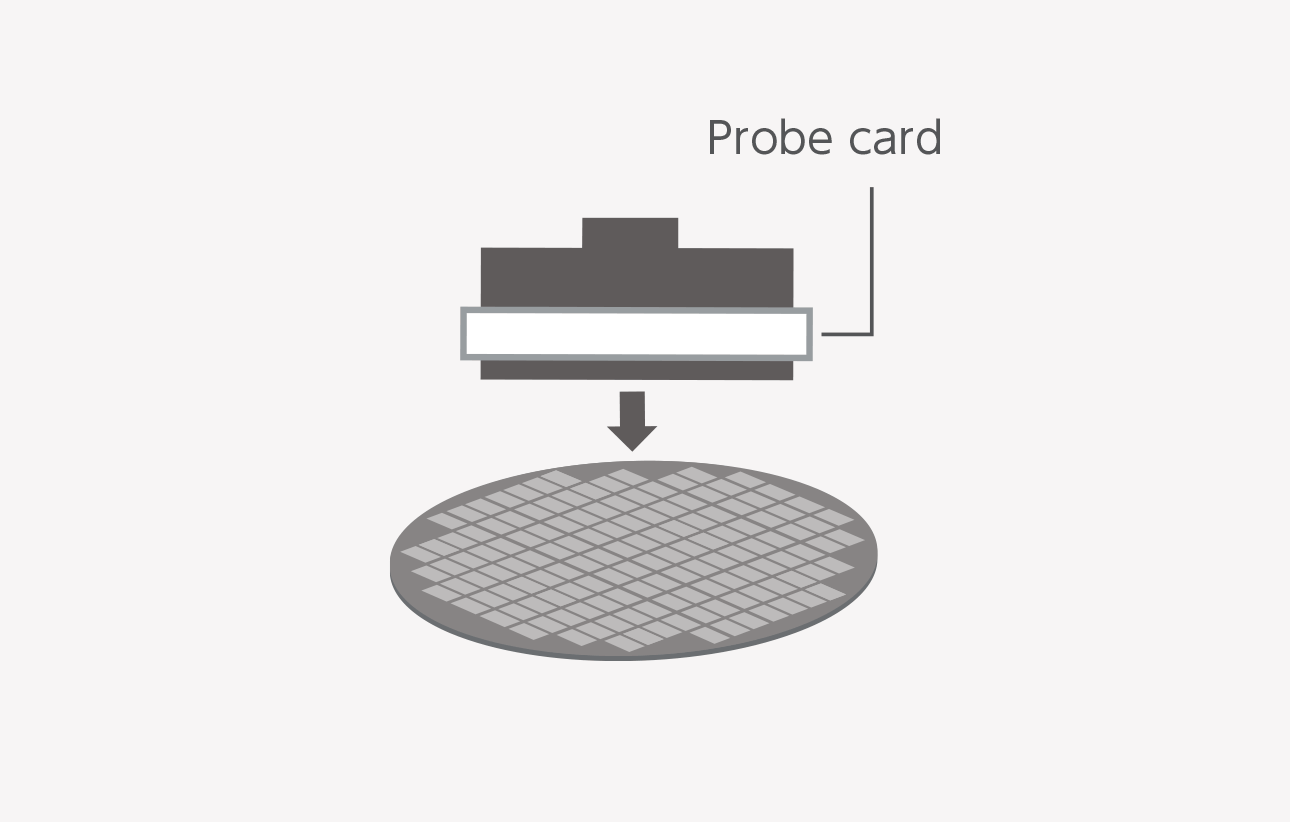
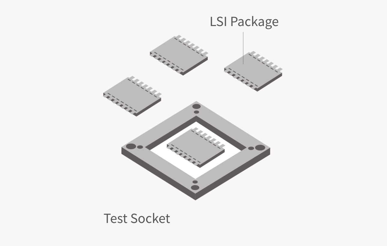
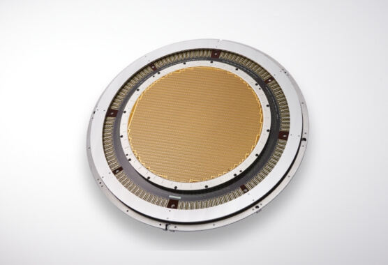
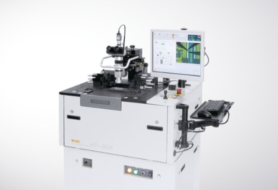
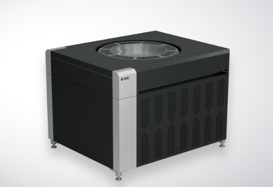
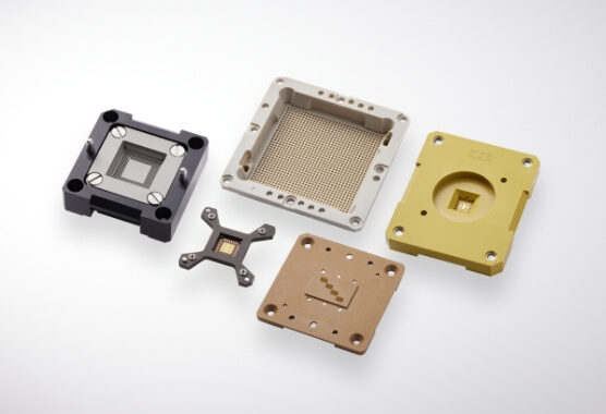
Our product lineup for the semiconductor manufacturing process includes probe cards for testing the electrical properties of wafers, testing equipment called IC testers and test sockets for property testing after packaging, as well as a wafer prober, which is used for evaluation and analysis during R&D of devices. As the functionality and diversity of semiconductors advances, we are supporting the enhancement of productivity and quality with our highly reliable testing and measurement technologies.
Applied Product Field
-

PC
-

Smart Phone
-

Server
-

Automobile
-

Game
Semiconductor Manufacturing Process
Select a process to see details
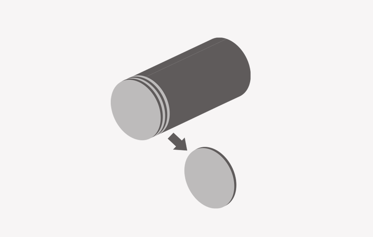
- Wafer manufacturing
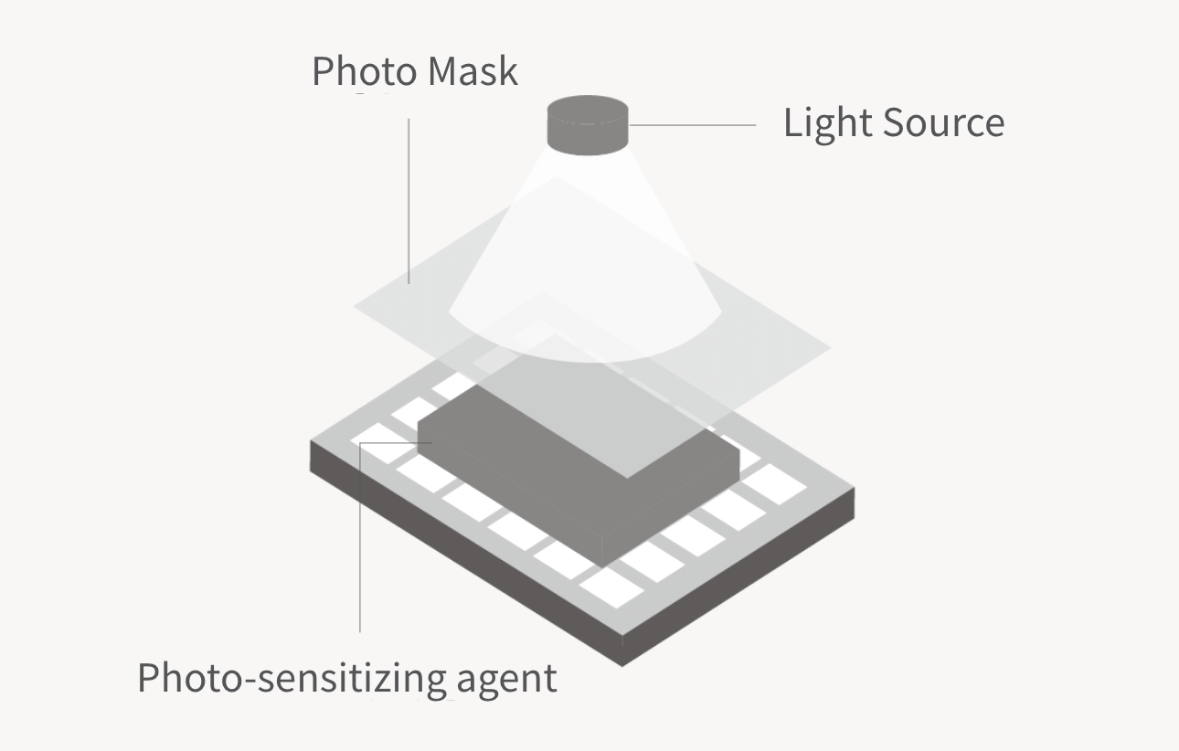
- Board wiring process
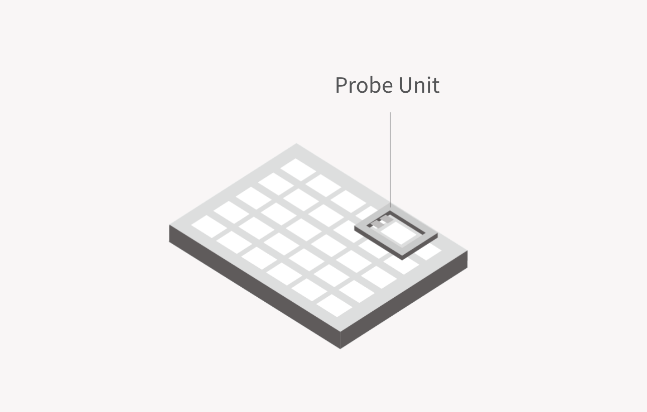
- Wafer testing
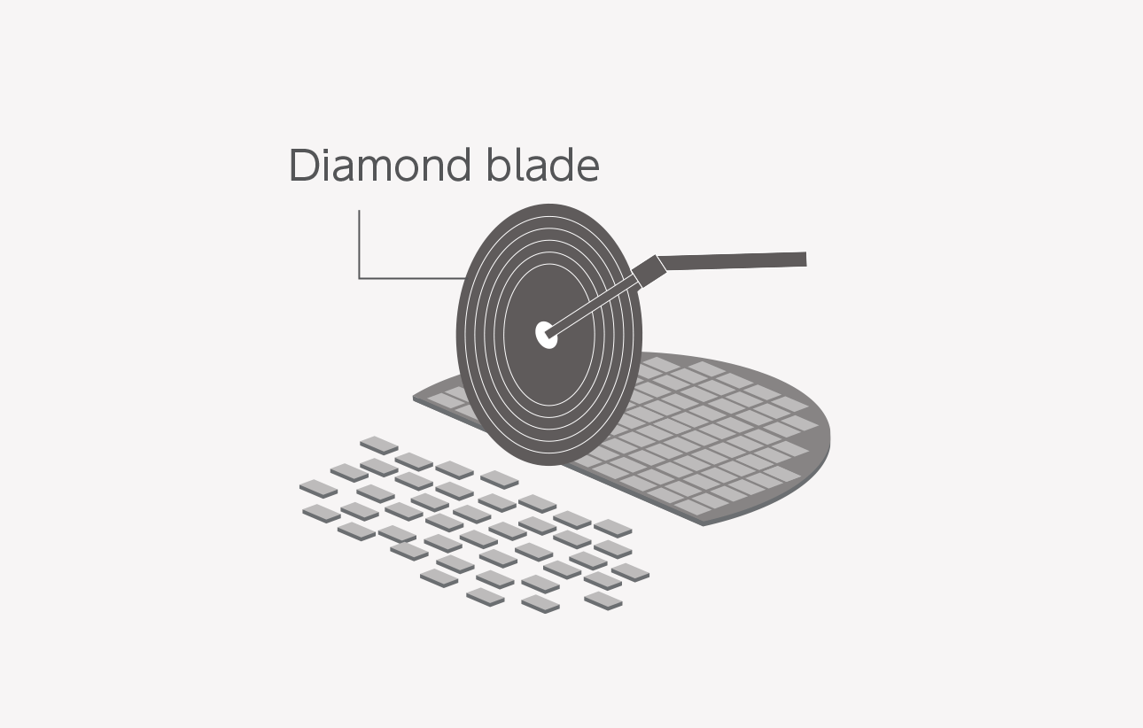
- Mounting and assembly process
- Final inspection

Products used in this process
Products used in this process
FPD Division
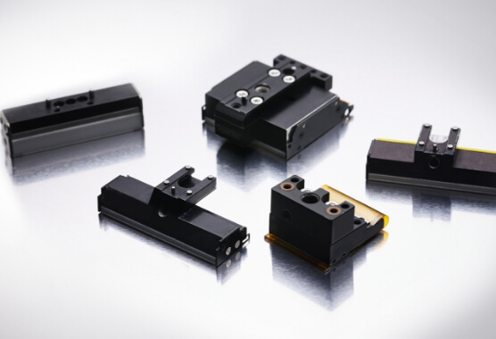
In the FPD field we offer products which are used for testing the electrical properties of flat panel displays (FPDs), and probe units that send electrical signals to test panels. As FPDs become larger with higher definition and more versatile, we are providing optimal testing solutions and contributing to productivity gains.
Applied Product Field
-

TV
-

Laptop
-

Tablet
-

Car Navigation
FPD Manufacturing Process
Select a process to see details
- TFT array process
- TFT array testing
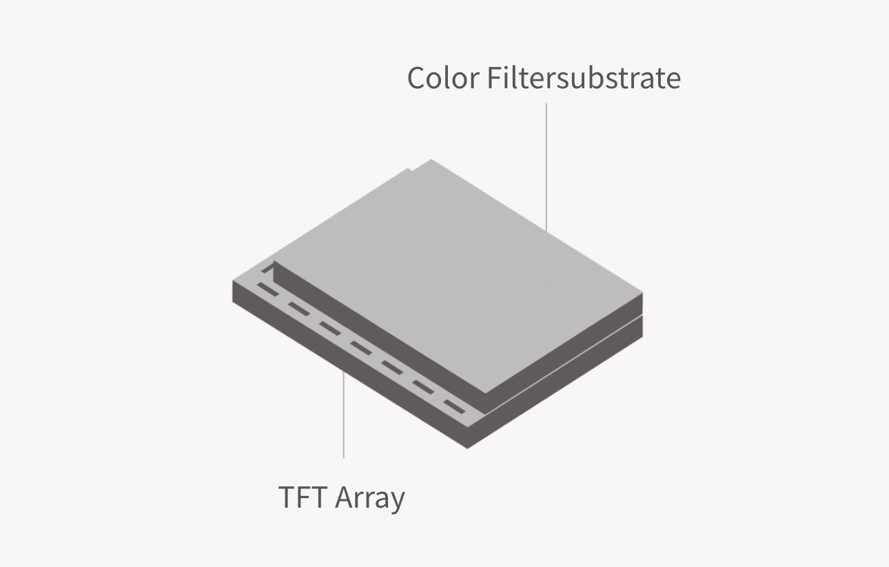
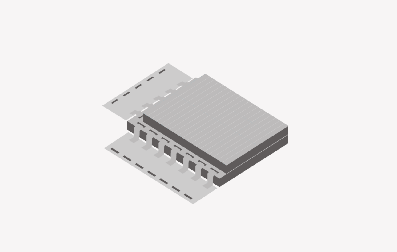
- Cell process
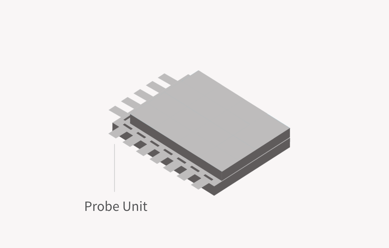
- Cell panel testing
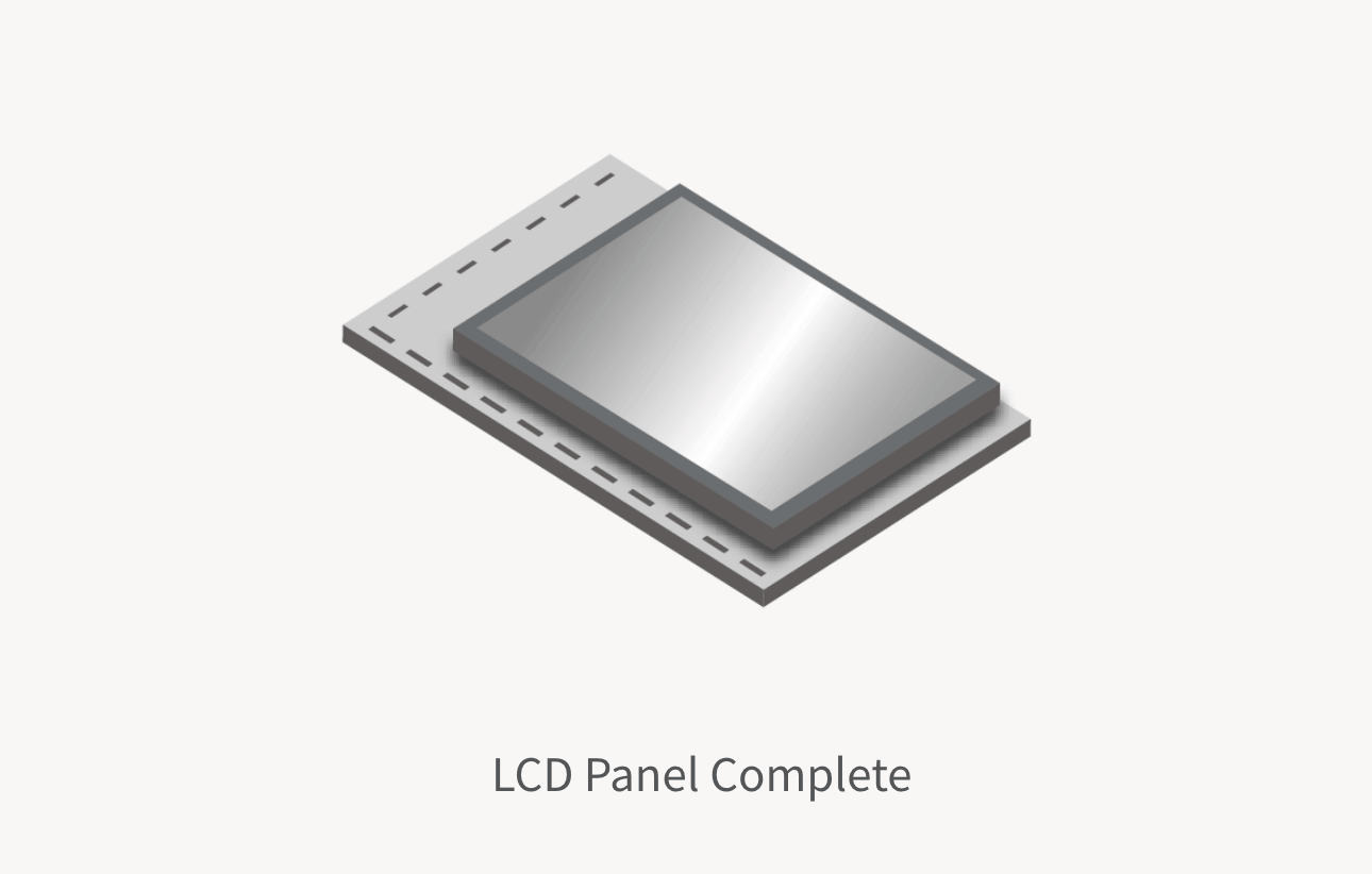
- Module process・testing
- Final inspection