Glossary
- A
- B
- C
- D
- F・G
- I
- L
- M
- N・O
- P・Q
- S
- T・V
- W・Y
A
Advanced Probe Card
A general term for advanced probe cards with narrow pitch and high pin counts that have superior electrical properties, and probes that utilize MEMS technology.
Amorphous
A material characterized as amorphous is a non-crystalline solid. Metals, non-metals and semiconductors in an amorphous state do not have the orderly atomic arrangement of perfect crystals. Amorphous silicon has semiconductor properties and can form films more easily than crystalline materials, so it is used for thin-film transistors (TFTs) for FPDs.
Area array
An arrangement with the terminals of IC surface-mount packages and the pads of IC chips arranged in a grid pattern.
Array Process
A process to form a TFT array on a glass substrate by the repetition of film forming, photolithography, etching, and other processes.
Array Test
An array test is conducted to test a TFT array. In the array test, a contact with the panel drives the gate lines to supply voltage to the pixels. The presence of any defects in the pixel circuit and wiring is checked by measuring the potential or electric charge of the pixels.
ASIC
Application specific integrated circuit
Assembly and Testing Process
In the LSI manufacturing process, the assembly and testing process is conducted after the wafer process (diffusion process) in order to dice wafers into chips and assemble the chips into packages.
B
Bare Chip
Bare chips are semiconductor IC chips diced from wafers and not yet packaged.
BGA
A ball grid array (BGA) is a type of surface-mount packaging. In order to allow surface mounting on printed circuit boards, BGA packages have a grid array of metal balls or metal bumps, which act as external connection terminals, on their base surface.
BIST
A built-in self-test (BIST) is a mechanism for design for testability (DFT). BIST of integrated circuits facilitates testing of ICs with high speed and a high pin count.
Bonding Pad
The supply of voltage to chips and transmission of signals from chips are normally conducted via lead. The term “bonding pads” refers to metal electrodes placed on the periphery of chips for the purpose of connecting the lead wires and inner terminals.
Bump
Solder protrusions set on the IC electrodes to provide contact between the circuit board and chip package, such as flip-chips.
Burn-in
A process to detect initial failures of semiconductors by testing them under extreme conditions such as high temperatures and voltages.
C
Cantilever-Type Probe Card
A type of probe card that conducts probing using probe needles, one end of which acts as a fulcrum.
CCD
A charge-coupled device (CCD) is a device that has the metal-oxide semiconductor (MOS) structure with numerous transmission electrodes arranged on an oxidized film on the silicon substrate surface. It features self-scanning and memory functions. CCD products include area sensors (solid-state image sensing devices) using photodiodes, linear sensors, and signal delay elements.
Cell / Cell Panel
A panel consisting of a TFT array substrate and a color filter substrate joined together with liquid crystal materials injected into the space between the two substrates.
Cell Process
A process where an array substrate and a color filter substrate undergo alignment treatment to align the direction of the liquid crystal molecules, and then liquid crystal is injected into the space between the two joined substrates.
Chip / Die
Dies and chips are small semiconductor devices. A semiconductor wafer is diced into many pieces, and each of these pieces is called a die or chip.
CMOS Image Sensor
A CMOS image sensor is a solid-state image sensing device using a complementary metal-oxide semiconductor (CMOS). Like a CCD image sensor (image sensing device), a CMOS image sensor uses photodiodes (PD), but its manufacturing process and signal readout method are different. With an amplifier for each cell, a CMOS image sensor reduces electrical noise in reading out electrical signals after photoelectric conversion.
COF
A chip-on-film (COF) package is an ultra-thin IC package where an IC chip is mounted on a film-like circuit board.
COG
“Chip-on-glass” (COG) refers to packaging where an IC chip is mounted directly on a glass substrate for LCDs, packages with photoelectric conversion devices, or other products using glass substrates.
Color Filter
A color filter, comprising a glass substrate and color resists, is used to create color images on an LCD screen. Most typically, one pixel is composed of red (R), green (G) and blue (B) sub-pixels, each enclosed by black lines of black matrix (BM). The RGB pattern is repeated in a grid.
CSP
A chip-size package (CSP) is a type of surface-mount packaging. In CSP packages, the size of the package substrate, onto which an IC chip is mounted, is the same as the IC chip in order to increase the mounting density.
D
DFT
Design For Testability is a design methodology involving the integration of testable features in large-scale ICs, reducing test times whilst improving fault detection rates.
DRAM
Dynamic random-access memory (DRAM) is a type of volatile memory. It is used widely as general-purpose memory as well as a computers' main memory.
DUT
Device under test
F・G
Final Test / Package Test
Electrical testing of assembled ICs.
Flip chip
Flip chips have bump electrodes on the chip surface for the purpose of high-density surface mounting of IC chips on circuit boards. The bumps and wiring board terminals are connected with solder or conductive adhesive.
FPD
Flat panel display
GaN
Gallium nitride
I
IC
Integrated circuit
IGBT
An insulated gate bipolar transistor is a power semiconductor device used to control electrical power. With the combination of a Metal Oxide Semiconductor Field Effect Transistor (MOSFET) for the input and a Bipolar Transistor for the output, it provides comparatively higher speed switching and high efficiency.
IGZO
IGZO is a transparent semiconducting material, consisting of indium, gallium, zinc, and oxygen, used in the backplane of LCDs and OLED displays. Compared to LTPS (low-temperature polycrystalline silicon), IGZO has higher mobility, leading to ultra thin displays and higher resolutions. The low off-current in TFTs means it is possible to achieve lower power consumption.
Impedance
The ratio of the applied voltage to the current. It is calculated by dividing voltage by current and expressed in units of ohm (Ω).
L
LCD
Liquid crystal display
Lighting Test
A lighting test is conducted to check the panel operation. A test pattern is displayed on the display screen to check for the presence of dot defects, line defects, or mura (unevenness). The lighting test can be a visual inspection by an operator or automated panel inspection using a CCD camera.
Liquid Crystal Display
These have the flowing properties of liquid whilst retaining the electro-optical properties of crystals. Liquid crystal displays employ liquid crystals as optical shutters.
LSI
“LSI” is a general term for large-scale integrated circuits. LSIs with a higher scale of transistor integration are called very-large-scale integrated circuits (VLSIs) and ultra-large-scale integrated circuits (ULSIs).
LTPS
Low-temperature polycrystalline silicon (LTPS) is polycrystalline silicon that has been synthesized at low temperatures of 600°C or lower. LTPS can be synthesized on a glass substrate and therefore its manufacturing cost is lower than that of high-temperature polycrystalline silicon.
M
MCU
A microcontroller unit (MCU), also called a single-chip microcomputer or microcontroller, is a small computer on a single integrated circuit containing a central processing unit (CPU), RAM, ROM, input/output (I/O) interface circuits, etc.
MEMS
Microelectromechanical systems is the technology of microscopic devices incorporating both mechanical parts (sensors and actuators) and electronic circuits into silicon or glass substrates, or into organic materials by way of microfabrication technology.
MEMS Type Probe Card
A probe card formed using MEMS technology for probe terminals.
Microcomputer
An IC that integrates a memory unit and/or communication functions with an external device (I/O) with a microprocessor for arithmetic operations on one chip. Recently, the word “microcomputer” is often used to refer to those incorporated in home appliances or other products for electronic control.
Mixed Signal
The term “mixed signal” refers to an integrated circuit that has both analog circuits and digital circuits.
Module Process
A process in which a driver IC, wiring, backlight unit, etc. are mounted on a cell panel.
MOSFET
A metal-oxide-semiconductor field-effect transistor (MOSFET) is a transistor that controls current between the source and drain with voltage applied to the gate electrode.
Mura
Mura, meaning “unevenness” in Japanese, refers to unevenness in display. Recognition of mura is influenced by unevenness in brightness or chromaticity, contrast difference, area, and other factors, as well as by the visual characteristics of the human eye.
N・O
NAND-Type Flash Memory
A type of non-volatile memory that retains data even without an external power source. Used in devices such as SD cards, USB flash drives, cellular phones, and auxiliary storage in computers.
NOR-Type Flash Memory
NOR-type flash memory is a type of non-volatile memory that can retain data without a power supply. Like random access memory (RAM), NOR-type flash memory allows access with address specification for reading, which is impossible for NAND-type flash memory. The NOR type features data reliability and does not require error-correcting code (ECC), which the NAND type needs. Therefore, the NOR type is used for microcomputers, routers that require superior reliability, printers, GPSs and firmware for in-car devices and other devices where the use of a hard disk is not possible.
OLED (Organic Light Emitting Diodes)
Organic EL displays are displays using organic light-emitting diodes. “EL” stands for electro-luminescence. Features of organic EL displays include high contrast, a wide viewing angle, and a short response time.
P・Q
Peripheral
These are parts of the device that are located on the four sides of IC packages, IC chip bonding pads, or test pads.
Pixel
A pixel is a functional unit of a display or imaging device. In color displays, one pixel is comprised of red (R), green (G) and blue (B) sub-pixels.
QFP
A quad flat package (QFP) is a type of surface-mount packaging with leads extending from each of the four sides of the package.
S
SBD
The Schottky barrier diode (SBD) is a diode using a Schottky barrier, which is created by a metal-semiconductor junction, and features high switching speeds.
Semiconductor
Semiconductor materials have electrical conductivity between that of conductors such as metals, through which current passes easily, and insulators such as glass, through which hardly any current can pass. Semiconductors have the properties of allowing or not allowing the passage of current with the application of voltage, light, heat, etc.
SiC
Silicon carbide (SiC) is a compound of silicon and carbon. This semiconductor material is used for high-power devices. SiC helps achieve high-voltage devices with very low on-resistance.
SoC / System LSI
The terms “system on chip” (SoC) and “system LSI” refer to a large-scale IC that integrates most of its functions, which have conventionally been achieved with combinations of multiple ICs, onto a single chip and therefore helps achieve small-sized high-performance devices. An SoC mainly consists of a processor, memory, input/output circuits, interface circuits, and communication circuits.
SRAM
Static random-access memory (SRAM) is called “static” because it does not need to be periodically refreshed to retain its data, unlike dynamic random-access memory (DRAM). SRAM can retain data for a short period of time, but data is lost when the power supply is lost. SRAM is used in applications such as CPU cache due to its high-speed read and write capabilities.
Surface Mount
Surface mount, or surface mount technology (SMT), is a method for placing or mounting ICs and electronic parts onto the surface of printed circuit boards.
T・V
TEG
A group of individual elements such as capacitors, transistors, and wirings in semiconductor IC chips and FPD array circuits that are tested to evaluate manufacturing processes and design verification. To do this, the elements' properties are tested using parametric testers or network analyzers.
Test Pattern
In semiconductor testing, the term “test pattern” refers to electrical signals input to validate IC operation. A test pattern is generated based on test specifications. DUT output is monitored and compared against the expected value to analyze test results. In an FPD test, the test pattern is the screen display for checking display quality. Red, green, blue, white, black and a gray tone are displayed on the screen to detect dot defects, line defects, and mura (unevenness).
TFT
A thin-film transistor (TFT) is a type of field-effect transistor. Its applications include pixel circuits for FPDs.
TFT Array
In LCDs and OLEDs pixels are arranged in a matrix, and TFTs for driving each of these pixels are also arranged in a matrix. Normally, these TFTs are formed on a substrate, which is called a TFT array. A pixel circuit consists of TFTs, pixel electrodes, and other elements, as well as gate wires for driving TFTs and signal wires for transmitting voltage to be supplied to the pixels.
Vertical Probe Card
A vertical probe card is a probe card in which probe needles are vertical to the substrate. Vertical probe cards are suitable for area array, small pad, low voltage, low needle pressure, and high frequency measurement.
W・Y
Wafer
Serving as a disk-shaped substrate, a wafer is a thin slice cut from a cylindrical crystal of silicon (Si), gallium arsenide (GaAs), or other material. Semiconductor electronic circuits are formed on the surface of a wafer.
Wafer Test/Probe Test
An electrical test conducted by placing a probe needle on a wafer chip bonding pad.
Wire Bonding
A method of electrically connecting bonding pads on the IC chip surface to packaging leads by using metal wires, etc.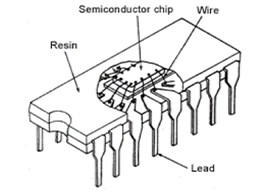
WLCSP
A wafer-level chip-size package is a chip-size package (CSP) that has had its components such as circuitry, terminal formation, and protective film coating attached before the wafer is diced.
Yield
The percentage of non-defective products.